


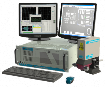
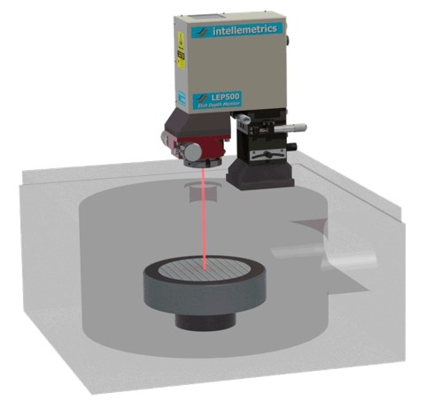
LEP500 Etch Depth Monitor 刻蚀深度监控仪
For Precision Etching 用于精密刻蚀
该仪器提供实时刻蚀深度监测,具有良好的噪音印制和降低生产或研发的设置成本。 该系统包括一套基于人性化的Windows输入,控制和可视化界面。EtchDirector 软件实时计算刻蚀速率和刻蚀深度在最苛刻的情况下增强对工艺终止的控制。
The LEP500 is designed to operate either as a standalone tool, or to be integrated into an OEM etch tool through a simple and robust communications interface.
LEP 500 可以做为一个标准的工具或通过一个简单和强大的通讯接口集成到OEM的刻蚀机上。
Overall Measurement Performance 测量的性能
Accuracy & Precision Depends upon etch process conditions 准确性和精度根据客户工艺条件不同而异.
Example Process : Etch Rate = 100 nm min-1, sample rate = 5 Hz
例如:刻蚀速率= 100 纳米/分钟, 样品速率 = 5 Hz
Intrinsic Etch Depth Accuracy本征刻蚀深度准确性: ± 0.67 nm
Intrinsic Etch Depth Precision本征刻蚀深度敬慕: ± 0.17 nm
· Real time, in-situ measurement and control 实时,在线测量和控制
· Predictive modelling software – reduce material waste & process development time 预测建模软件 — 减少材料浪费和工艺开发时间
· Data reprocessing mode to decrease process optimisation time 数据在处理模式,减少工艺优化时间
· Integration to etch tool for automated operation可以集成在刻蚀机上,实现自动化操作
· Fast data acquisition and high noise rejection for accurate termination 快速的数据采集和高噪音抑制获得准确的终点
· Operates in Interferometry AND Reflectometry modes 在干涉测量或反射模式下操作
· Monitors etch proceeding through bulk layers, doesn’t rely on material interfaces监控刻蚀工艺通过散装层,不依赖于材料的界面
· User friendly Windows driven interface – fast and intuitive 人性化的Window 驱动界面—快速和直观
· Remote control for through-wall cleanroom implementation 可以实现洁净室穿墙远程控制
Application 应用领域
Materials 材料: III-Vs, Dielectrics, Polymers, Silicon, Metals, II-VIs;
Processes 工艺: RIE ICP Vapour Etch;
Sectors 类别:Optoelectronics, Optics, Failure Analysis, Photomask, III-V Electronics, MEMS;
EtchDirector软件 - Powerful, Intuitive Windows-based Interface 基于Windows 强大,直观的界面
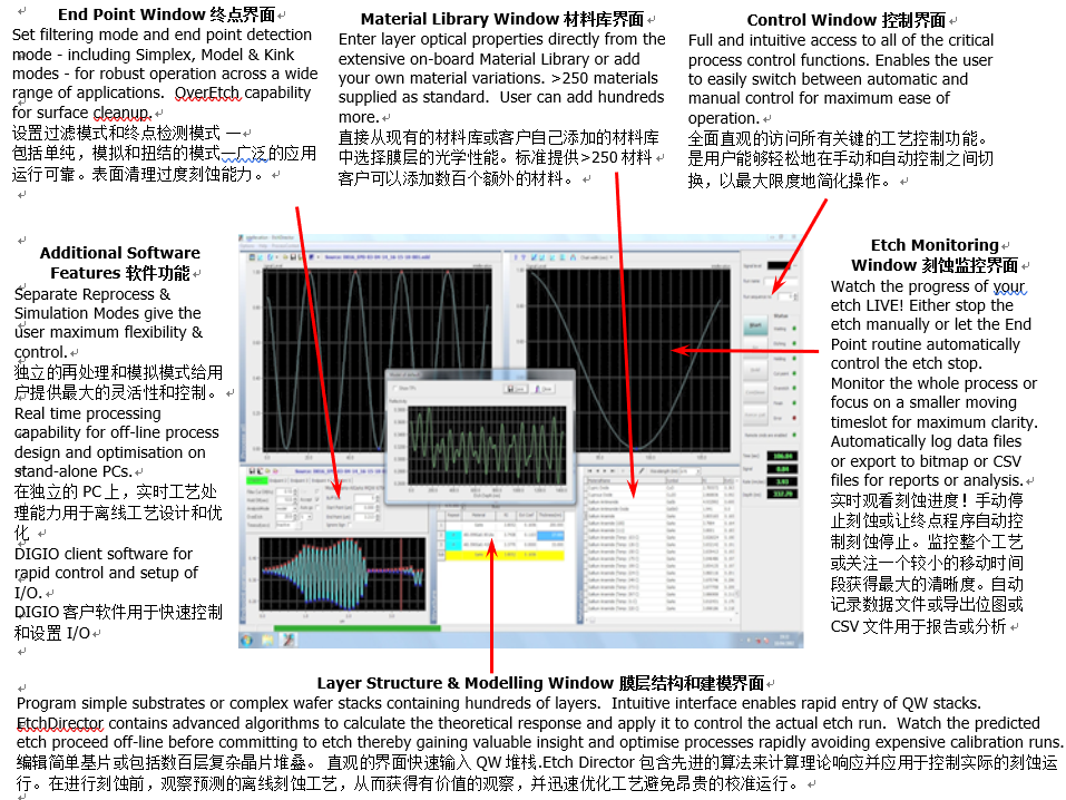
|
Enhanced
Spot Size and Vision System 增强光斑大小和视觉系统
Laser Spot Size = 8mm to 25mm depending upon working distance 激光光斑尺寸 = 8微米到25微米 根据工作距离不同
Standard Camera Resolution= 1280 x 1024 (higher resolutions available on request 标准相机分辨率:1280 x
1024 (可提供更高分辨率的相机)
Image Viewing Features 图像显示特点:
· Gain: Auto or manual lock 增益:自动或手动锁定
· Exposure time: Auto or manual lock 曝光时间:自动或手动锁定
· Contrast: Auto, manual, over a defined area 对比:自动,手动,在规定的区域内
· Edge Enhancement 边缘增强
· A range of zooming and resizing options 一系列缩放或调整大小的选项  | |
典型客户名单: OEMs: Oxford Instruments Plasma Technology, UK;SPTS, UK; Trion Tech, USA;Samco, Japan; JLSDesigns, UK; PlasmaTherm, USA; Advanced Vacuum, Sweden;Cello Technology, Taiwan; Elettrorava, Italy; End Users: Glasgow University, UK; Compound Semiconductor Technologies, UK; Sheffield University, UK; Toshiba Research, UK; Sandia Labs, USA; University of California Santa Babara, USA; University of New Mexico, USA; JDSU, USA; Lockheed Martin, USA; Lumentum, USA; NRC, Canada; Chalmers University, Sweden; Institut fur Mikro- und Nanotechnologies, Switzerland CNRS-LPN, France; CNRS-IEMN, France; Ikar-Impulse, Russia;Tyndall Institute, Ireland |
 苏公网安备32050802010865号